


TrendForce 2026 San Francisco Roadshow arrives October 16. Join us to unpack how advanced packaging is reshaping the foundry industry, alongside the latest AI server and data center market dynamics, and what they mean for the future of global AI infrastructure: REGISTER HERE.
Advanced packaging has become one of the most closely watched battlegrounds in the AI chip supply chain. Back in May, we took a close look at some of the key bottlenecks, including SeWaRe micro-cracking in glass substrates and warpage in panel-level packaging. The industry is moving fast. TSMC continues to expand CoWoS capacity aggressively, while reportedly developing an “EMIB-like” approach of its own. Meanwhile, Intel’s EMIB-T has reportedly seen a significant yield improvement, intensifying the rivalry between the two advanced packaging heavyweights.


Against this backdrop, TrendForce maps out the latest developments in 2.5D and 3D advanced packaging, from the architectural differences between EMIB and CoWoS, to capacity trends, customer distribution, and what comes next as the industry moves toward panel-level packaging, glass substrates, and 3D stacking.
Chiplet Architecture: It All Comes Down to Interconnects
To understand why advanced packaging has become so critical, it helps to start with how chip design has been evolving.
As semiconductor nodes continue to shrink, transistor architecture has evolved in parallel. For instance, when semiconductor technology moved from 28nm to 16nm, the industry shifted from planar transistors to the FinFET (Fin Field-Effect Transistor) architecture. The next major transition begins at 2nm, marking the start of the GAAFET (Gate-All-Around FET) era.
Although the CFET (Complementary FET) architecture has already been developed for sub-1nm nodes, the cost of process scaling continues to climb. In response, IC designers have begun adopting a disaggregation strategy, breaking a single chip down into multiple chiplets. This means components that do not require extreme scaling are separated out, and only the core portions of the chip are shrunk further.
Realizing the full potential of a chiplet design depends on the interconnect quality between dies, which is precisely where advanced packaging comes in. By packing chiplets tightly together, advanced packaging enables high-bandwidth, low-latency interconnects.
Related report: The 2026 Semiconductor Inflection Point: Scaling from 2nm GAA to the Era of ASIC Sovereignty
2.5D Packaging: EMIB vs. CoWoS
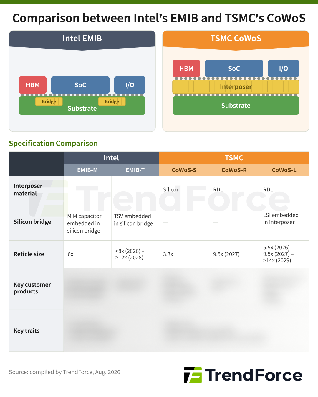
CoWoS (Chip-on-Wafer-on-Substrate) is TSMC’s 2.5D advanced packaging technology. It integrates two sequential processes: CoW (Chip-on-Wafer), in which multiple dies are bonded onto a silicon interposer via micro-bumps, and oS (on-Substrate), in which the interposer is subsequently bonded onto the package substrate.
At 2026 OCP APAC Summit, TSMC stated that its 5.5x reticle size CoWoS is now in volume production, with yields consistently topping 98% across multiple AI customer products and reaching as high as 99% in some cases. The company expects to scale beyond 14x reticle size by 2029.
The key difference between Intel’s EMIB and CoWoS lies in the interposer. EMIB embeds a silicon bridge directly into the substrate to serve as the communication link between chips, eliminating the need for a full-size interposer and reducing cost as a result.
Assuming comparable yield stability between the two, Intel’s EMIB architecture offers lower cost potential than TSMC’s CoWoS by design. As for reticle size, Intel previously noted that its EMIB-T will scale to more than 8x this year and beyond 12x by 2028.
Although performance and reliability at scale have yet to be fully validated, the technology has already attracted interest from major ASIC vendors. At its 2026 Q2 earnings call, Intel CEO Lip-Bu Tan said the company is now focused on ramping EMIB-T into high-volume production to support customer ramps in 2027.
Taiwan’s OSAT providers have also been moving quickly in 2.5D packaging. ASE’s Fan-Out Chip on Substrate (FOCoS) uses multiple RDLs to integrate processors, memory, and I/O chips, with RDL layer counts scaling from 3 or 6 layers up to as many as 12. According to the company, this delivers interconnect density roughly 50x that of traditional flip-chip packaging, and over 200x with FOCoS-Bridge. SPIL, meanwhile, has developed FOEB (Fan-Out Embedded Bridge), which embeds silicon bridges within the RDL layer to enable near-monolithic, high-density, short-reach connections between dies.
Related report: Foundry Market Bulletin - Aug. 17, 2026
Behind the paywall, we explore:
EMIB vs. CoWoS full spec comparison and key customers
CoWoS capacity share among major customers
Updates on glass-based solutions and 3D/3.5D packaging
TrendForce view on overall supply and price trends