

Glass Substrates Are Breaking Through the AI Chip Packaging Bottleneck
Intel's No SeWaRe Result Signals Mass Production One Step Closer. Plus Key Players and Supply Chain Opportunities

The AI infrastructure buildout is often discussed in terms of chips and computing power. But beneath the surface, a set of supply chain bottlenecks is quietly shaping the pace and cost of deployment. Last week, we looked at glass fiber cloth. This week: glass substrates.
Related report: T-Glass Supply Shortages: AI Rack Fiberglass Trends
As AI chips grow more complex, package sizes keep expanding, and traditional organic substrates are reaching their limits. Under high temperatures during assembly, warpage reduces yield and becomes increasingly difficult to manage as package sizes grow.
Against this backdrop, glass, with better thermal and mechanical properties, is emerging as the next-generation material for advanced packaging. Glass-based solutions fall into two categories: one replaces the core layer of the substrate with glass, known as a glass core substrate; the other replaces the silicon interposer with glass, known as a glass interposer.
Intel has been an active mover in glass substrate technology. As early as 2023, Intel committed to glass substrates in its advanced packaging roadmap. In January 2026, it debuted the first sample combining EMIB packaging with a glass core substrate at NEPCON Japan — achieving No SeWaRe, or no micro-cracks — marking a decisive step toward commercial reality.
Meanwhile, Samsung and Rapidus are expected to roll out glass interposer solutions, while SK Absolics is targeting mass production of glass substrates in 2026.
This article covers the technical advantages of glass substrates, the manufacturing challenges that remain, and how the supplier landscape is taking shape.
Bigger Chips, Bigger Packaging Problems
As AI computing power requirements increase, the size of a single AI chip package is gradually expanding. Although ASML’s EUV (0.33 NA) currently limits the maximum reticle size to 26×33 mm (approximately 830 mm²), TSMC uses mask stitching technology to join multiple reticle patterns together in order to increase chip size.
Related report: Global AI Server & Supply Chain Outlook 2026
The single‑package size of NVIDIA’s Blackwell GPU is about 3.3× reticle size, roughly 2,739 mm². The next‑generation Rubin GPU is expected to expand to 4× reticle size, about 3,320 mm², while the Rubin Ultra GPU will reach 9× reticle size, about 7,470 mm². In addition to NVIDIA, Google’s TPU v9x (HumuFish) is also expected to adopt a large size of 9.5× reticle size.
According to TSMC’s CoWoS reticle size roadmap, the 5.5× reticle size variant is currently in mass production, with 9.5× targeted for 2027, 14× for 2028, and beyond 14× planned for 2029. Intel, meanwhile, is targeting a 12× reticle size EMIB solution by 2028 to address the demand for larger chip packages.
But scaling up package size introduces two key challenges.
First, square chips are increasingly hard to fit efficiently onto round wafers, which increases wasted area at the wafer edges. This led to the concept of panel‑level packaging (PLP), which uses square panels instead of round wafers, and is able to raise area utilization to over 75%.

Second, if large packages continue to use organic core substrate (mostly ABF materials made by laminating resin, glass fiber cloth, and copper foil), warpage during the reflow heating process becomes more severe, thereby reducing overall integration yield. (A deeper analysis of warpage challenges will be covered in our next article.)

Therefore, glass, which is flat in surface and is close to that of silicon (Si) in coefficient of thermal expansion (CTE), has become an ideal replacement for organic materials as an interposer or substrate.
Why Glass Substrates Outperform Organic Substrates
Simply put, better thermal, electrical, and physical properties.
CTE close to silicon: Organic core substrates (OCS) have a CTE of roughly 7 ppm/°C, a significant mismatch with silicon’s 2.6 ppm/°C that could easily cause warpage. Glass, with a CTE of 3-9 ppm/°C, can be matched to silicon, maintaining stable yield even in large-size packages.
Excellent dielectric performance: Glass is an excellent insulator. At 10 GHz, its dielectric constant (Dk) can be as low as 2.5-6, and its dielectric loss (Df) can be as low as 0.0005-0.005, allowing it to maintain signal integrity even in high‑speed transmission applications.
Flat and smooth surface: Glass has extremely high surface flatness and smoothness, allowing it to achieve finer line width/spacing (L/S), such as <2 µm.
, dielectric loss (Df), and through-hole density.")
, dielectric loss (Df), and through-hole density.")
 and glass core substrates (glass with metal and polymer layers), showing structural differences in advanced chip packaging.")
Who Is Building What, and When
As glass materials have excellent properties for advanced packaging, major foundries and OSATs are adding new product lines that use glass as either substrates or interposers.

TSMC unveiled its 310×310 mm CoPoS (Chip-on-Panel-on-Substrate) product line in 2025, and plans to establish a first mini production line at VisEra in 2026, begin small‑volume trial production in 2027, and reach mass production between 2028 and 2029. TSMC uses glass as an interposer in CoPoS, which requires a thinner profile (approximately 400 µm, roughly half the thickness of a substrate) and stricter CTE requirements, making it technically more challenging than glass used as a substrate.
Note: CoPoS replaces the traditional round glass carrier with a square panel format, improving interposer (RDL) utilization rates and eliminating the edge and corner area loss. (Updated June 2026)
Samsung announced at CES 2024 that it is developing glass interposer technology. In 2025, it established its first mini production line through SEMCO for glass core substrates, with mass production scheduled for 2027. Rapidus, meanwhile, showcased the largest glass interposer sample to date — measuring 600×600 mm — at SEMICON Japan 2025, with mass production targeted for 2028.
SK Group’s Absolics, a joint venture with Applied Materials, had already invested about KRW 300 billion in 2022 to build the first glass‑substrate factory in Covington, Georgia. Its goal is to develop glass substrates that can directly embed active/passive components, eliminating the interposer to reduce package area, thickness, and power consumption. The substrate measures 510×515 mm, with mass production planned for 2026.
Intel has been particularly active in glass substrate development. In September 2023, at Innovation Day, it announced plans to use glass substrates for advanced packaging, with mass production targeted between 2026 and 2030. On January 22, 2026, at NEPCON Japan, Intel showcased its first sample combining EMIB packaging with a glass core substrate. The package measures 78×77 mm (approximately 1,716 mm²), supports 2× reticle size, and uses a 10-2-10 stack structure (10 RDLs + 2 glass core layers + 10 RDLs, 22 layers total), with a total thickness of 800 µm and a bump pitch of 45 µm. Intel also reported achieving “No SeWaRe” (no micro-cracks) in testing, marking a decisive step toward mass production.
One Big Hurdle in Mass Production: SeWaRe
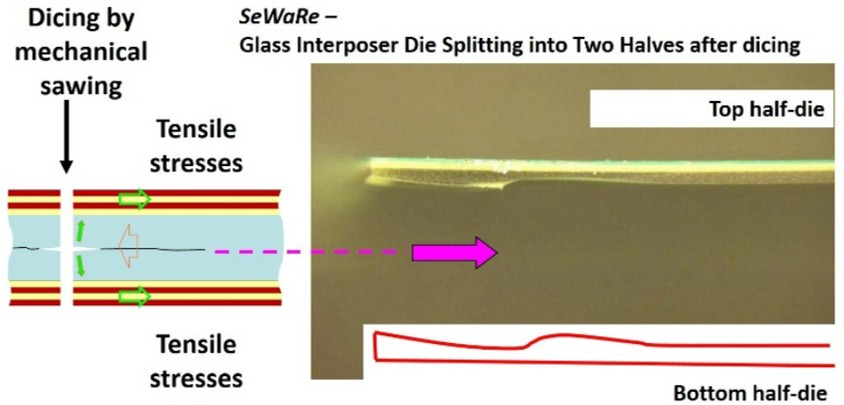
The biggest mass‑production challenge for glass substrates is “SeWaRe.” SeWaRe comes from the Japanese term 背割れ, meaning “back crack,” and refers to micro‑cracks that form during processing, especially drilling and dicing. As glass is brittle, micro‑cracks, once they appear, become stress‑concentration points that can cause the glass substrate to break during later testing and packaging steps.
As illustrated below, SeWaRe caused by dicing easily leads to near mode I fracture failure, which refers to the phenomenon where a material, under normal (perpendicular) stress, splits into upper and lower halves and fractures.
To reduce the probability of SeWaRe occurrence, the current mainstream glass substrate fabrication process includes:
Through-Glass Via, TGV: Typically, laser modification is first performed inside the glass, and then selective wet etching is applied to the modified regions to form TGV. TGV are X-shaped, because tapered sidewalls are better at distributing stress.
Polymer Lamination: A resin buffer layer is laminated onto the glass surface. Since copper (Cu) has a relatively high CTE, about 17 ppm/°C, the resin buffer layer prevents direct contact between the copper and the glass, avoiding cracking during thermal expansion and contraction.
Seed Sputtering: A metal seed layer is sputtered onto the surface.
Plating: A conformal metal layer is electroplated on the surface of the seed layer to reduce the amount of copper, and thereby prevent cracking during thermal expansion and contraction.
The process then repeats steps 2-4 according to the required number of layers to complete the multilayer structure.

During multilayer processing, the resin layer can still shift due to thermal expansion and contraction, causing tensile stress on the glass. A study by Shinko Electric Industries found that applying a resin edge coating on the glass substrate reduces edge stress. For example, a 300μm-thick resin layer creates about 95MPa of stress on the glass, but with edge coating, the stress can be reduced to about 49MPa.

To resolve the SeWaRe issue, various suppliers across the glass substrate process flow are actively rolling out solutions. For instance, Germany’s LPKF has introduced LIDE technology for TGVs. This technology involves laser-induced modifications followed by selective wet etching to form holes. Japan’s DISCO has launched its SD and LEAF laser dicing technologies, while Onto Innovation has released the Firefly G3, a metrology system for TSV inspection.
Supply Chain Dynamics
Currently, major semiconductor equipment and materials for glass substrate manufacturing are dominated by leading companies from Europe, the United States, and Japan. For instance, LPKF supplies TGV equipment; SCHOTT, Corning, AGC, and NEG provide low-CTE glass; Lam Research supplies etching and plating systems; DISCO specializes in dicing equipment; Onto and KLA offer inspection tools; and SUSS and EVG provide temporary bonders and debonders.
Glass substrate technology is advancing on multiple fronts. For a comprehensive analysis of key players and supply chain opportunities, access the full report: Intel's No SeWaRe Glass Substrates: TGV Challenges and Advanced Packaging Supply Chain Role
In addition to advanced packaging, glas substrates also have a pretty unique application in the photoics world.
https://arvindsrinivas.substack.com/p/know-your-glass-complexity-and-importance
What makes this transition important is that advanced packaging is quietly becoming as strategically critical as transistor scaling itself.
For years, the industry narrative revolved around process nodes.
Now the bottlenecks are shifting toward integration complexity:
substrates, interposers, thermals, power delivery, and yield engineering.
The semiconductor stack is becoming a systems engineering challenge far beyond just lithography.