


As test-time scaling takes hold, the focus of the AI industry is quickly shifting from training to inference. NVIDIA, Google, and other major AI players rolled out inference-specific chips in the first half of 2026, while AI ASIC startups such as Cerebras, SambaNova, and Etched have announced new products and strategic partnerships. Alongside this shift, the memory hierarchy is undergoing structural change, with vendors turning to HBF, SSD POD, and SRAM to push past the capacity and bandwidth limits of conventional HBM.
This piece is written for readers looking to build a clear, foundational understanding of AI memory requirements.
Contents:
Memory requirements for AI training
Memory requirements for AI inference
How the memory structure changes as the industry moves from training to inference

Memory Requirements for AI Training
AI training refers to the process of using a training dataset to teach an AI model new capabilities. AI inference refers to the process of applying an already-trained model to new data to generate a response. Because these two stages require very different types of memory, memory architecture has diversified rapidly in recent years.
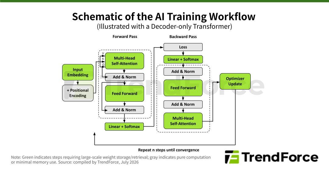
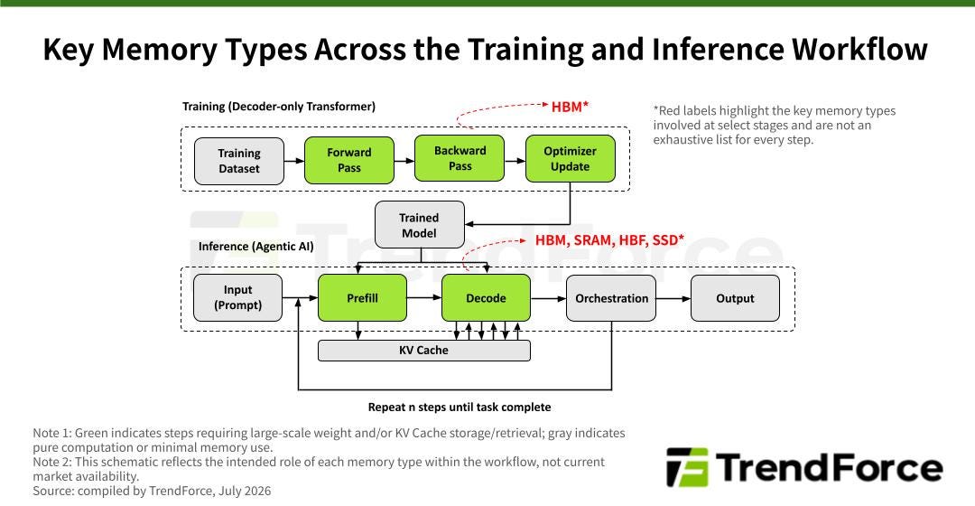
Taking today’s dominant Transformer architecture as an example, the training process consists of three main stages:
Forward Pass: The weights of each layer are read from memory into the compute die, where large-scale matrix multiplication produces a predicted output. A loss function then compares this output against the correct answer to measure the error (loss).
Backward Pass: Following the chain rule, the model reads the activations temporarily stored during the forward pass, layer by layer, and computes gradients that match the size of the weights.
Optimizer Update: After reading the gradients, the model updates and writes back the weights themselves, along with two optimizer state tensors of the same size as the weights (first-moment m and second-moment v).
Because the model must repeat these three stages over and over to minimize loss and converge, memory access speed becomes the key factor determining training efficiency.
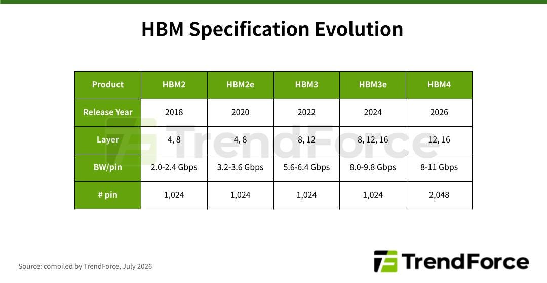
This is the context in which HBM (High Bandwidth Memory) emerged: multiple layers of DRAM stacked vertically and connected via TSV. Unlike conventional DRAM, which connects over relatively slow PCIe (PCIe 6.0 x16 offers 128 GB/s of unidirectional bandwidth), HBM is packaged side by side with the compute die on the same interposer, shortening the data path. A single HBM stack can deliver more than 2 TB/s of bandwidth (HBM4 offers over 1 GB/s per pin in one direction across 2,048 pins), which has significantly accelerated the industrialization of AI.
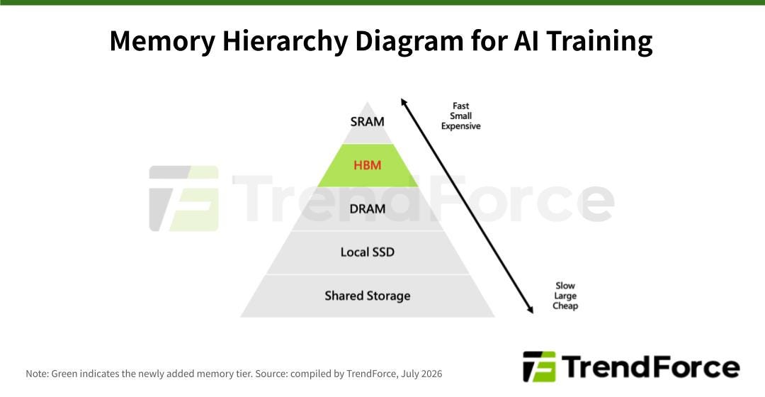
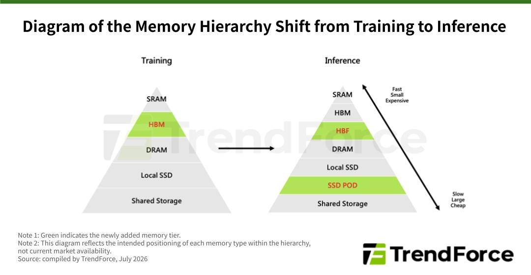
The memory hierarchy gained a new tier, HBM, during the training era, filling the gap between on-chip SRAM and conventional DRAM.
Related report: 3Q26 HBM Datasheet
Memory Requirements for AI Inference
AI inference consists mainly of two stages:
Prefill: The input prompt is processed in parallel in a single pass. The Key and Value vectors for each layer are computed and stored in memory (the KV Cache), and the first output token is generated at the same time.
Decode: Key and Value vectors are read from the KV Cache to generate tokens one at a time, while newly computed Key and Value vectors are continuously written back into it, until the response is complete.
Because the Decode stage requires repeated token-by-token reads and writes to the KV Cache, and because KV Cache size keeps growing with the number of conversation turns, context window length, and batch size, relying on HBM alone is increasingly insufficient to keep up with growing inference demand. Memory capacity has become a second critical bottleneck, alongside bandwidth.
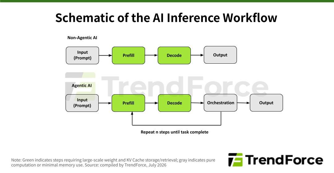
Unlike the relatively mature memory architecture built for AI training, AI inference memory architecture is only now developing rapidly alongside test-time scaling. Vendors are still actively experimenting with different memory approaches, and the memory hierarchy is in the middle of a paradigm shift.
To address the growing capacity needs of KV Cache, memory makers SanDisk and SK hynix announced a partnership in August 2025 to develop HBF (High Bandwidth Flash), which stacks multiple layers of NAND vertically and connects them via TSV. At an expected bandwidth of 1.6 TB/s, a single HBF stack is projected to offer around 512 GB of capacity, roughly ten times or more that of HBM (a 16-Hi HBM4 stack offers 48 GB), filling the gap between HBM and conventional DRAM.
While HBF has yet to reach mass production, many vendors are concurrently using KV Cache offloading to move less frequently used KV Cache down to lower tiers of memory, easing the burden of storing large volumes of KV Cache. In this context, NVIDIA introduced the concept of SSD POD in 2026, filling the gap between local SSD and shared storage.

Notably, beyond HBF and SSD POD, some inference ASIC startups have introduced high-speed SRAM to break past HBM’s speed limits. Groq (whose inference technology license and core team were secured by NVIDIA in December 2025) and Cerebras, for example, use large areas of on-chip SRAM to significantly increase decode speed.
Related report: 2026 Trends: Memory for New AI Inference Demand
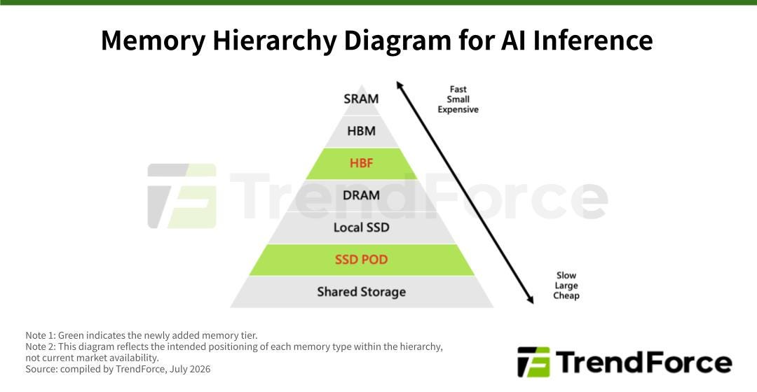
Memory Structure Changes from Training to Inference
In the first half of 2026, as inference demand continued to surge, NVIDIA announced it will incorporate the Groq LPX chip into its Rubin series, expected to be available later this year, alongside the introduction of CMX (Context Memory Storage Platform) and the Vera CPU Rack.
Google also unveiled the TPU v8i, designed specifically for inference, which carries 72 GB more HBM3e and 384 MB more SRAM than the TPU v8t, which is designed for training.
Beyond these two major players, a number of AI ASIC startups building inference-specific chips have been active in the first half of 2026: SambaNova launched its fifth-generation chip, the SN50, in February 2026; Cerebras filed for an IPO in April 2026 and announced partnerships with OpenAI and AWS; and Etched announced in June 2026 that its Sohu chip had successfully taped out at TSMC.

Looking at how the training era was dominated almost entirely by HBM, compared with the far more varied inference landscape today, the design choices for the memory hierarchy can be expected to keep diversifying going forward.
Coming up next
In our next piece, we take a closer look at how industry leaders are turning to CXL expansion and KV Cache compression to address the memory bottleneck, along with what this means for the memory market going forward. Subscribe so you don’t miss it.
HBM solved a bandwidth problem. KV cache makes inference a capacity problem too, so HBF and pod-level context storage look more like new tiers than simple replacements.