


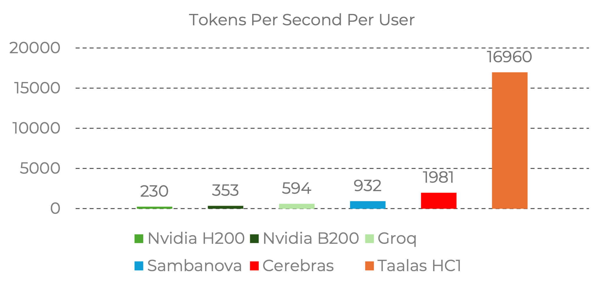
On December 24, 2025, Nvidia secured Groq’s inference technology license and core team for $20 billion. Two months later, on February 20, 2026, Canadian AI chip startup Taalas unveiled its inference chip HC1, achieving 16,960 tokens/sec per user on the Llama 3.1 8B model, approximately 48 times that of the Nvidia B200 under equivalent conditions. On May 14, 2026, Cerebras officially went public, once again drawing market attention to the AI inference chip sector.
From Nvidia’s multi-billion dollar bet and the wave of startup launches to capital markets beginning to price these companies, it is clear that in the AI inference era, industry competition has shifted from building “bigger” models to “more efficient” models. This article will explore:
The trend of AI shifting from training toward inference
Architectural bottlenecks of general-purpose GPUs
Advantages and challenges of hard-coded inference chips
An overview of high-efficiency inference chip startups
Related report: NVIDIA FY1Q27 AI Server Outlook: GB/VR Rack Leads
Industry Shift: From Training to Inference
In the early days of generative AI’s rise in 2022, industry competition focused on model training. Whoever could train the most powerful model held the competitive edge, leading companies to pour massive capital into stacking parameters and chip resources in pursuit of leaps in model scale and capability.
However, as AI services enter routine deployment, the cost structure has changed. Unlike training, which is a high-capital but low-frequency R&D expense, inference is a high-frequency, long-term cost directly tied to revenue. Cost per token and energy efficiency directly affect gross margins and the ability to scale. Every API call and every generated token represents compute consumption and margin pressure. If token generation costs cannot decline with scale, the sustainability of the business model comes into question.
Consequently, the focus of hardware and software development has shifted toward throughput, energy efficiency, and memory architecture optimization, emphasizing data movement efficiency and low-latency design rather than simply pursuing peak compute performance.
Related report: NA CSPs Capex Surge Powers AI Infra Expansion
Architectural Bottlenecks of General-Purpose GPUs
Traditional general-purpose GPUs rely on HBM and external DRAM to store model weights, with compute cores physically separated from memory. Data must frequently move between the chip and the package. As inference traffic grows continuously, the architectural bottleneck of general-purpose GPUs becomes increasingly apparent.
For Transformer inference based on matrix multiplication, memory bandwidth and access latency are the primary constraints. While HBM provides high bandwidth, it comes with complex packaging, yield issues and high costs, and rising power consumption as bandwidth scales. For low-batch, low-latency requests, GPUs struggle to leverage their massive parallel advantage, leading to decreased utilization and higher costs per token.
On the other hand, as model scale is no longer the sole measure of competitiveness, the market has begun exploring ways to compress models while preserving inference capability. For example, 1.58-bit quantization and weight pruning enable models to maintain inference accuracy at extremely low memory footprints; Mixture-of-Experts (MoE) architectures reduce actual computation through a “partial activation” mechanism that activates only a small subset of expert sub-networks during each inference pass.
The rise of lean models opens a new direction for hardware design: when model weights and structure become stable and no longer require expensive dynamic memory to support flexibility, the path of embedding algorithms directly into silicon becomes commercially viable.
Related report: Crossing AI Memory Wall: Storage Layer Reallocation and HBF Analysis
Hard-coded Inference Chips: Advantages in Power, Cooling, and Capital Efficiency
Hard-coded inference chips emerged in response to efficiency bottlenecks. Vendors such as Taalas embed model weights in Mask ROM (Read-Only Memory) and use on-chip SRAM to handle dynamic data, drastically reducing the power consumed by external memory data movement and significantly improving tokens per watt and tokens per dollar. The primary benefits are low latency, low power consumption, and high throughput, with simplified cooling and packaging design.
However, the market’s primary concern remains hardware inflexibility in the face of rapidly evolving model updates. As a structural risk, specialized chips offer little room for adjustment compared to programmable architectures. Use cases must be highly stable and deployment scales sufficiently large to amortize non-recurring engineering (NRE) costs. The ecosystem also presents a meaningful barrier: cloud markets continue to rely on general-purpose platforms, and customers may prefer flexible solutions that can evolve alongside model upgrades.
To mitigate these risks, vendors are pursuing automated model-to-chip pipelines, pre-fabricated wafers, and hybrid programmable architectures integrating quantization and LoRA fine-tuning, striking a balance between hard-wiring and flexibility to enable commercial deployment.
Going forward, hard-coded technology is expected to gain traction in ultra-low-latency applications and closed-deployment scenarios where model structures are stable, privacy requirements are high, and deployment scales are well-defined. Hard-coded chips can operate in standard air-cooled racks, reducing energy consumption and capital expenditures, making them particularly attractive to cloud service providers and vertical integrators. Conversely, traditional ASIC vendors relying on software-compiled scheduling will face performance pressure at the architecture level.
Overall, TrendForce expects general-purpose GPUs to continue dominating training and multi-model environments. In mature, predictable inference scenarios, specialized architectures are expected to carve out their own space, not by displacing GPUs, but by addressing use cases where efficiency and cost structure matter most. The industry is thus evolving toward a dual-track structure where general-purpose and specialized computing coexist.
Taalas HC1: Proof of Concept for Hard-coded Inference
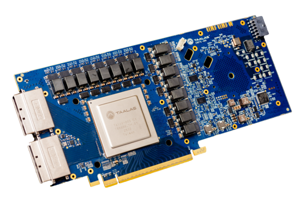
On February 20, 2026, Canadian AI chip startup Taalas launched the Taalas HC1, hard-wiring Llama 3.1 8B model directly into the chip, achieving a throughput of 16,960 tokens/s/user.
Moreover, the Taalas HC1 uses TSMC’s N6 process, requires no HBM memory or CoWoS packaging, and has a single-chip TDP of approximately 250W (air-cooled). Based on Taalas's analysis, compared to the Nvidia B200 (throughput optimized) running Llama 3.1 8B at a cost of 3.79 cents per million tokens, the Taalas HC1 achieves a cost of just 0.75 cents per million tokens, approximately one-fifth.
The key to Taalas’s compute efficiency lies in adopting the concept of Computing-in-Memory (CIM). CIM integrates compute functions within memory to perform computation directly within memory, eliminating the need for frequent data transfers between compute units and memory, thus removing the memory wall bottleneck, and reducing excess latency and power consumption during computation.
What is Computing-in-Memory? Since mathematician John von Neumann published the von Neumann architecture in 1945, chip design has followed a structure where components such as the Central Arithmetical (CA) unit and the Memory (M) unit are separate to maintain greater flexibility.
However, as the growth of memory bandwidth and computing power has become increasingly mismatched, the transfer of data between the computing unit and memory has become a major constraint. Computing-in-Memory (CIM) emerged to address this, evolving into various forms such as Digital CIM (DCIM), Analog CIM (ACIM), and Hybrid CIM. Nevertheless, the programming languages, underlying software architectures, and applications capable of running on CIM are not yet fully developed, and the technology remains in its early stages of development.
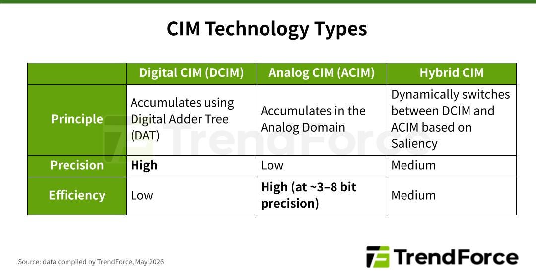
Compared to conventional CIM implementations, Taalas takes a more radical approach through hard-coding. Operating on the philosophy that “The Model is The Computer,” Taalas creates a fully hardware-defined AI hardcore model that embeds model weights directly into the chip’s Mask ROM. This captures the low-latency and low-power benefits of CIM while bypassing the bottleneck of CIM’s currently immature software ecosystem.
Beyond exceptional compute efficiency, by using high-density ROM to store model weights, Taalas can produce a dedicated chip for a new AI model by modifying just 2 mask layers — converting an AI model into a physical chip in just 2 months. Taalas also retains a portion of SRAM for KV cache and LoRA fine-tuning weights, compensating for the lack of flexibility.
Despite their different implementations, Taalas’s fully hardware-defined approach and Groq’s fully software-defined approach share the same goal: to achieve static scheduling and fully deterministic computation as much as possible, trading dynamic flexibility for maximum efficiency.
A New Era of Inference Chips: Diverse Technology Paths in Parallel
Beyond Taalas, a growing number of AI chip startups specializing in high-efficiency inference have entered the space, including Tenstorrent, Groq, Cerebras, SambaNova, MatX, Untether AI, Hepzibah AI, Etched, d-Matrix, Positron AI, Axelera AI, and FuriosaAI. Chip specifications across vendors are summarized below:
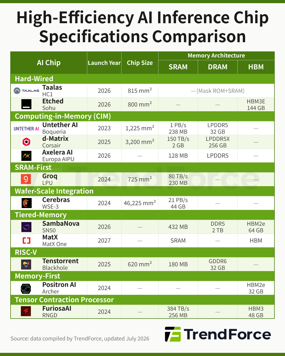
Implementation methods vary across Hard-Wired and CIM vendors. Taalas HC1 directly hard-wires model weights into Mask ROM (fully hardware-defined). Etched Sohu similarly uses a hard-wired architecture but applies to all Transformer models, offering greater flexibility. Within CIM: d-Matrix Corsair uses Digital Computing-in-Memory (DIMC) as its core technology, embedding the AI model’s underlying architecture into the chip, applicable to all AI models with even greater flexibility than Etched. Untether AI Boqueria uses at-memory compute, integrating RISC-V processors and processing elements directly within SRAM memory banks. Axelera AI Europa AIPU also uses Digital In-Memory Computing (D-IMC), with RISC-V controlling the data flow.
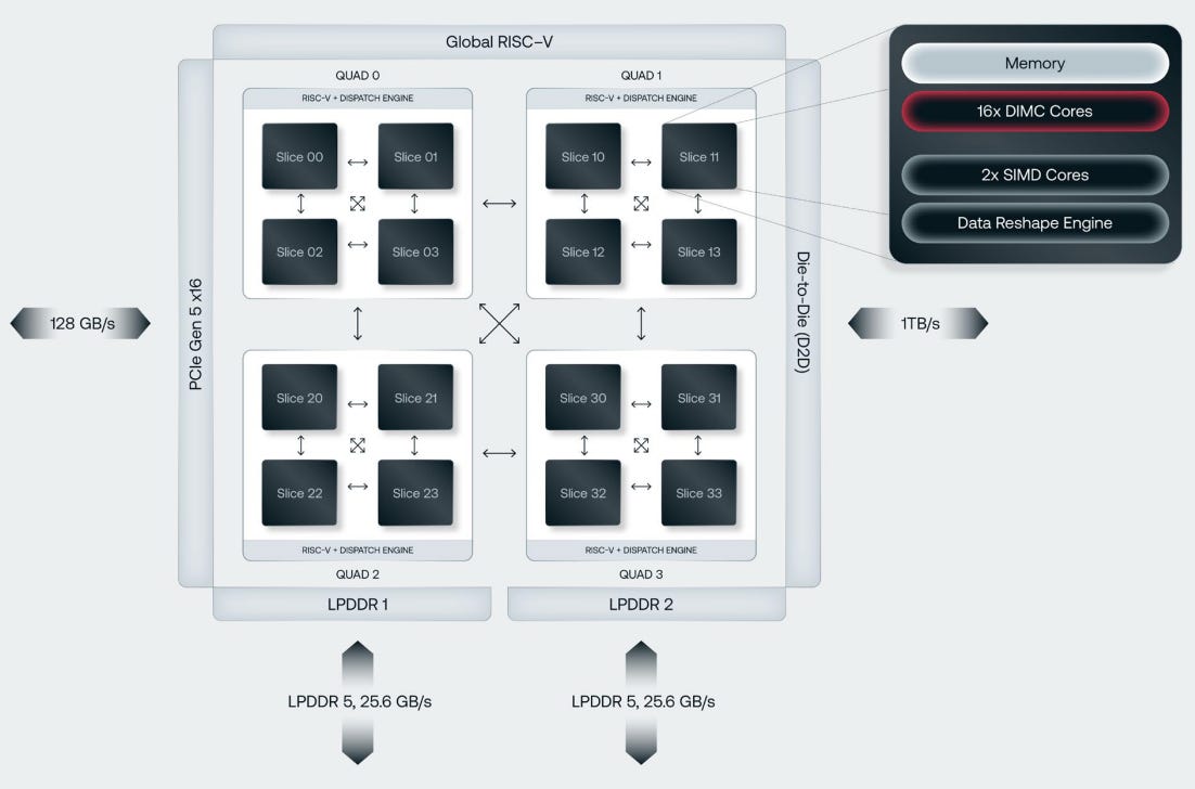
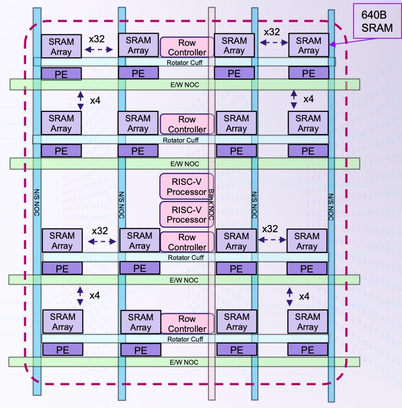
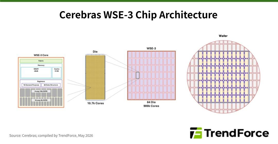
On May 14, 2026, Cerebras, currently the most talked-about name in the inference chip space, officially listed on the Nasdaq. Its core technology is Wafer-Scale Integration (WSI), which consolidates an entire 12-inch wafer into a single chip (WSE-3), delivering 44GB of on-chip SRAM and 21 PB/s of bandwidth. Cerebras has also secured a three-year compute partnership with OpenAI valued at over $20 billion and 750MW in capacity.
Currently, the market is in an early exploratory phase with multiple parallel tracks. Startups are simultaneously pursuing different technology paths, including Computing-in-Memory (CIM), SRAM-first architectures, wafer-scale integration, and tensor contraction processor. It is expected that future inference chip architectures will gradually integrate these various approaches to meet the performance and efficiency demands of AI inference.
Does 3D-DRAM be a better option for inference?
Anyone has any views on whether on chip models are good or bad? Basically what happens if at a future point of time, there are significantly better models making it largely inefficient to use the programmed model on the chip? Do you just bin the chip at that point or what lol?