


The fiber array unit (FAU) is a critical passive optical component in CPO. Precisely aligning and securing it onto an optical engine (OE) demands extremely stringent precision and directly affects yield and manufacturing efficiency. This step, known as FAU coupling, has become one of the key bottlenecks in CPO manufacturing and testing.

As CPO adoption expands from scale-out to scale-up, OE shipments are projected to grow significantly between 2027 and 2028, making the precision and capacity of the FAU coupling stage a key battleground for equipment vendors.
This article explains why FAU coupling has become a bottleneck and examines the equipment vendors competing to solve it, including ficonTEC, Suruga Seiki and TOYO Automation, GMT Global, All Ring Tech, and FitTech, along with key FAU, lens, and fiber suppliers.
Related report: CPO Technology Revolution: Next-Gen Interconnect for AI Data Centers
Two Coupling Paths for TSMC’s COUPE
At SEMICON Taiwan 2026, TSMC outlined an aggressive COUPE upgrade roadmap. Bandwidth per COUPE stands at 3.2 Tbps in 2026 and is expected to double to 6.4 Tbps by 2027, with a long-term target of exceeding 51.2 Tbps. TSMC also reiterated that integrating the OE onto the substrate can deliver 4X the energy efficiency of traditional copper interconnects and reduce latency to <0.1X. When the OE is further integrated onto the interposer (OOI), energy efficiency improves to 10X and latency drops to <0.05X.
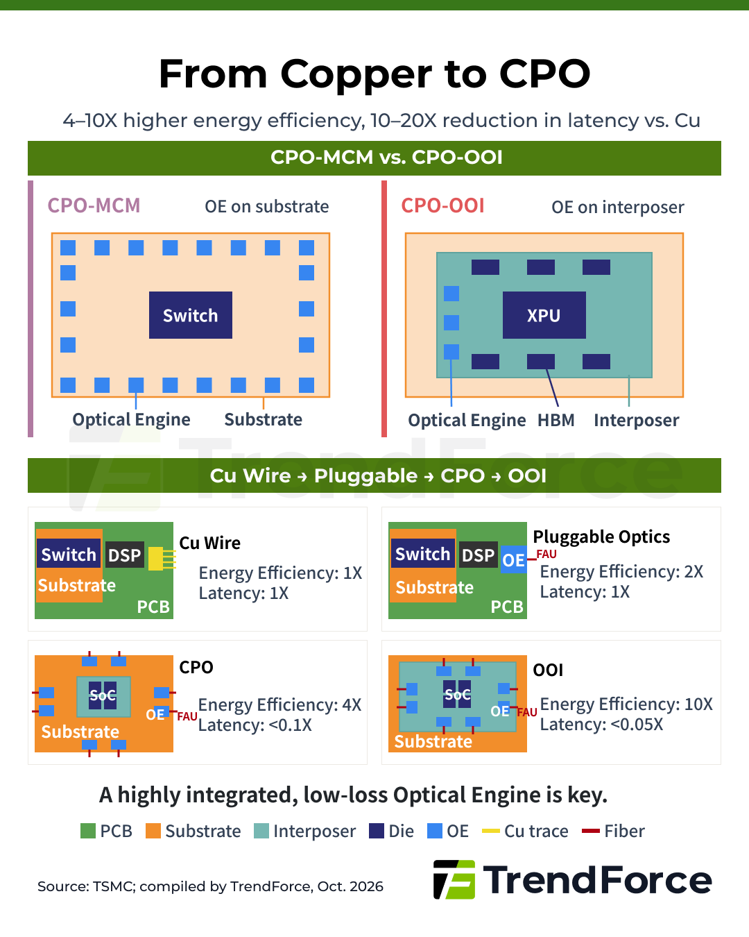
From pluggable optics to CPO and OOI, the optical engine has steadily moved from the PCB into the package and closer to the compute die. Along the way, the FAU, which connects the optical fibers to the optical engine, has become part of the packaging process.
The FAU is a highly precise passive optical component that serves as an interface between optical fibers and the waveguides on the PIC. Its primary function is to align and secure the fibers so that light can be precisely coupled into the waveguides. Depending on the coupling architecture, the optical path may further incorporate microlenses/microlens arrays (MLAs), or other optical elements.
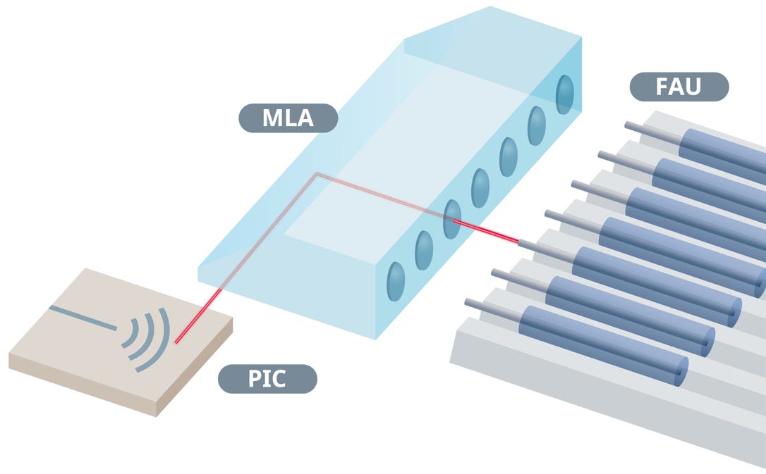
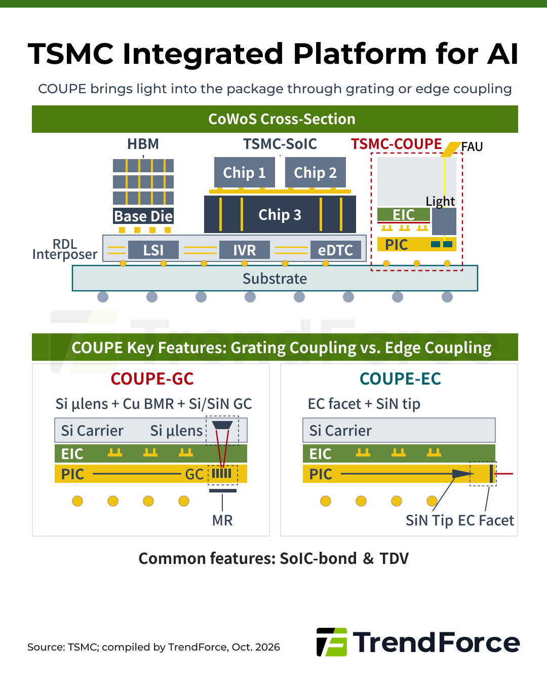
In silicon photonics chips, two of the most common ways to couple light between an optical fiber and the PIC are grating coupling (GC) and edge coupling (EC). A GC couples light in from the chip surface, which makes wafer-level optical testing easier, but it is typically more sensitive to wavelength and polarization. An EC instead guides light in through an optical facet on the side of the chip. It generally offers lower coupling loss and a wider operating wavelength range, but because the facet at the chip edge must be formed and accessed, wafer-level testing is more difficult.
TSMC’s COUPE supports both architectures. COUPE-GC combines a Si μlens, a Cu BMR (backside metal reflector), and a Si/SiN grating coupler to direct light into the PIC from above, while COUPE-EC couples light in from the side of the chip through an EC facet and a SiN tip. Both share common integration features, including SoIC bonding and TDV, and differ mainly in the optical coupling architecture between the fiber and the PIC.
Related report: 2026 New CPO Battleground: TSMC’s COUPE Roadmap Signals Opportunities for FAU Coupling Equipment
In the rest of this article, we break down why FAU coupling matters, why it has become a bottleneck, and how equipment vendors are positioning themselves in this market.