TrendForce Roadshow Japan 2026 takes place in Tokyo on December 8. Join us for insights on the next breakthroughs in foundry, DRAM, and HBM, how fast CPO will scale, and how custom ASICs and a split US-China market are reshaping the AI server landscape in 2027. REGISTER NOW.
Since HBM’s debut, it has been home turf for SK hynix, Samsung, and Micron. From the DRAM dies to the base die at the bottom of the stack, memory makers controlled both design and manufacturing. However, as HBM becomes one of the most critical components of AI chips, that division of labor is starting to change. By Marvell’s estimate, HBM now takes up roughly 30% of a typical AI accelerator’s die area and, at 2026 memory prices, more than half of XPU cost.
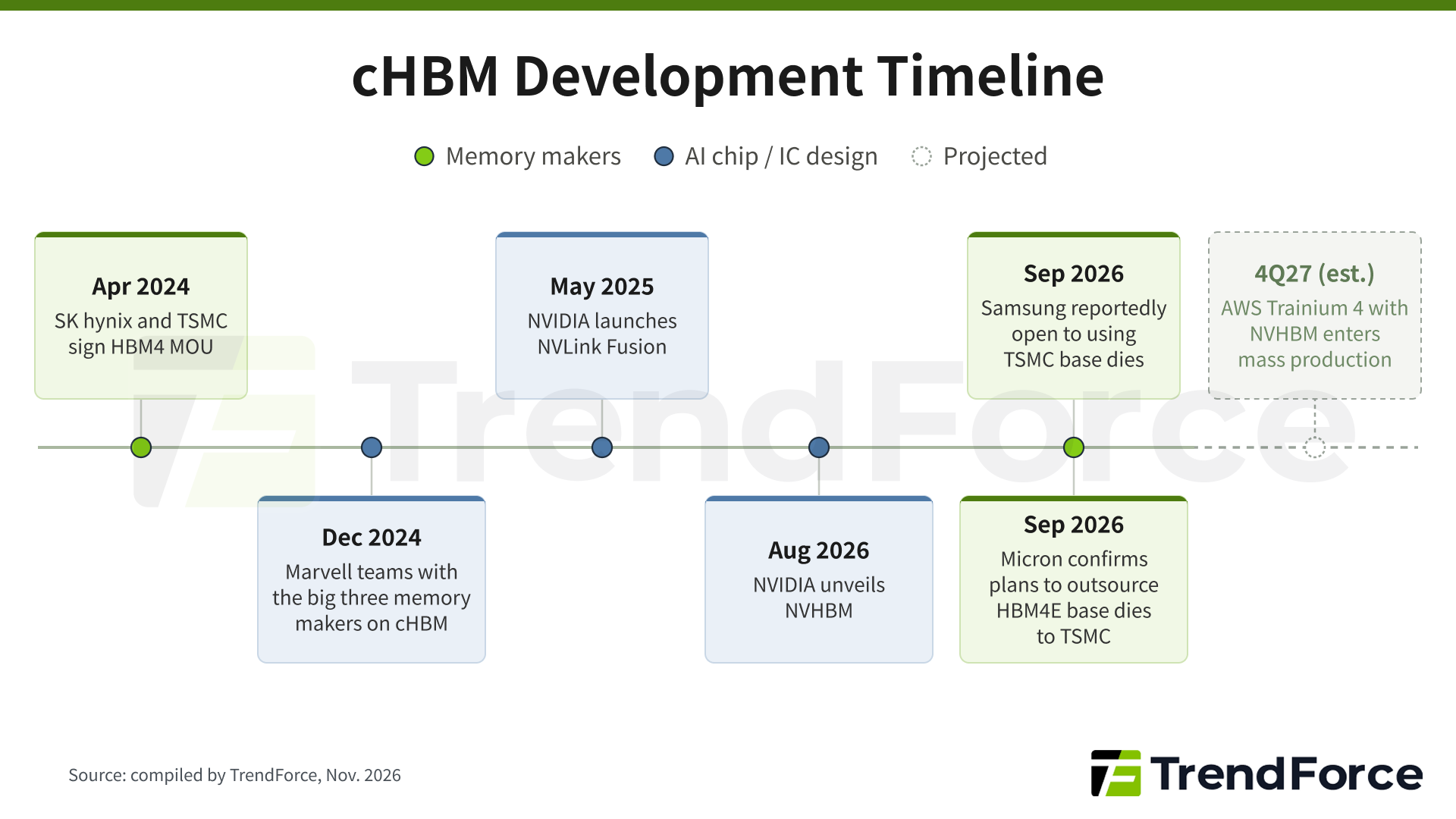
In August 2026, NVIDIA unveiled NVHBM, its Custom HBM (cHBM) platform integrated into the NVLink Fusion lineup, with deployment expected in AWS’s Trainium 4 and NVIDIA’s own Feynman GPU. In October, Marvell presented “Custom HBM as a System” at the OCP Global Summit, arguing that the base die, D2D interface, and package thermals must be co-designed as one system, and that “no single company can build custom HBM alone”: memory makers, foundries, OSATs, and XPU designers all need to be involved. With GPU and ASIC designers now helping define the foundation of HBM, cHBM appears to be on the final stretch toward mass production.
TrendForce observes that AI chip developers are actively evaluating cHBM, as standard HBM (sHBM) must prioritize compatibility, leaving limited room for optimization for individual accelerators. Meanwhile, the shift of base die production to advanced logic processes is expected to raise TSMC’s importance in the HBM supply chain.
Related report: Custom HBM Rises as Advanced Base Dies Elevate TSMC
Below, we break down:
Why the HBM base die is shifting toward advanced logic processes
How NVIDIA’s NVHBM is reshaping the HBM value chain
How SK hynix and Samsung are differentiating themselves at the base die level
Why TSMC’s role in the HBM supply chain is strengthening