


TrendForce 2026 Korea Roadshow takes place in Seoul on November 18. Join us for insights on how advanced packaging is reshaping the foundry industry, the next growth drivers for DRAM and HBM, and the emerging role of LPDRAM in next-generation computing. REGISTER HERE.
In our previous article on hybrid bonding, we looked at why it has become the key to getting past the scaling limit of micro-bumps, and why TSMC’s SoIC-X is expected to lift demand for hybrid bonders as its adoption in AI chips grows. The road from micro-bump to hybrid bonding, however, is not a single step. Hybrid bonding comes with high costs and demanding cleanroom requirements, so the industry is still seeking intermediate or complementary options along the way.

This is why other bumpless bonding technologies are drawing attention. SK hynix’s roadmap, published in August 2026, positions bumpless TCB as an interim step between fluxless TCB and hybrid bonding. This article looks at the bumpless options beyond hybrid bonding: how they work, how they differ, and how equipment suppliers are developing their strategies.
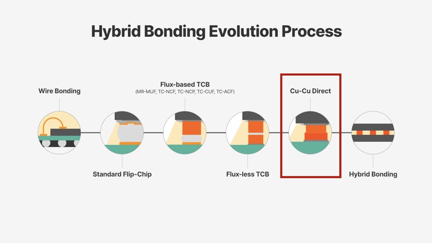
Why go bumpless
As bump pitch shrinks, bonding in advanced packaging has progressed from flip-chip, suited to bump pitches of roughly 50 µm, to micro-bump plus thermo-compression bonding (TCB). Fluxless TCB, which uses no conventional flux, now supports a bump pitch as small as about 8 µm. However, even as thermo-compression technology improves, the micro-bump itself still faces a physical scaling limit. This is what gave rise to bumpless bonding.
Bumpless means no conventional solder balls. Instead, metal on the chip surface, such as Cu pads or under-bump metal (UBM), makes direct contact, allowing smaller interconnects and a bond pitch that can reach around 5 µm. Hybrid bonding is currently the only commercialized bumpless technology. It bonds the dielectric layers and Cu pads of the chips directly through steps such as plasma activation and pre-bonding.
Behind the paywall, we explore:
What drives the cost of hybrid bonding
How bumpless flip-chip, bumpless TCB, and hybrid bonding compare
When memory makers could move to bumpless bonding
How die bonder suppliers are pursuing multiple tracks at once